
Innovative Technology Designs Start with the Right PCB
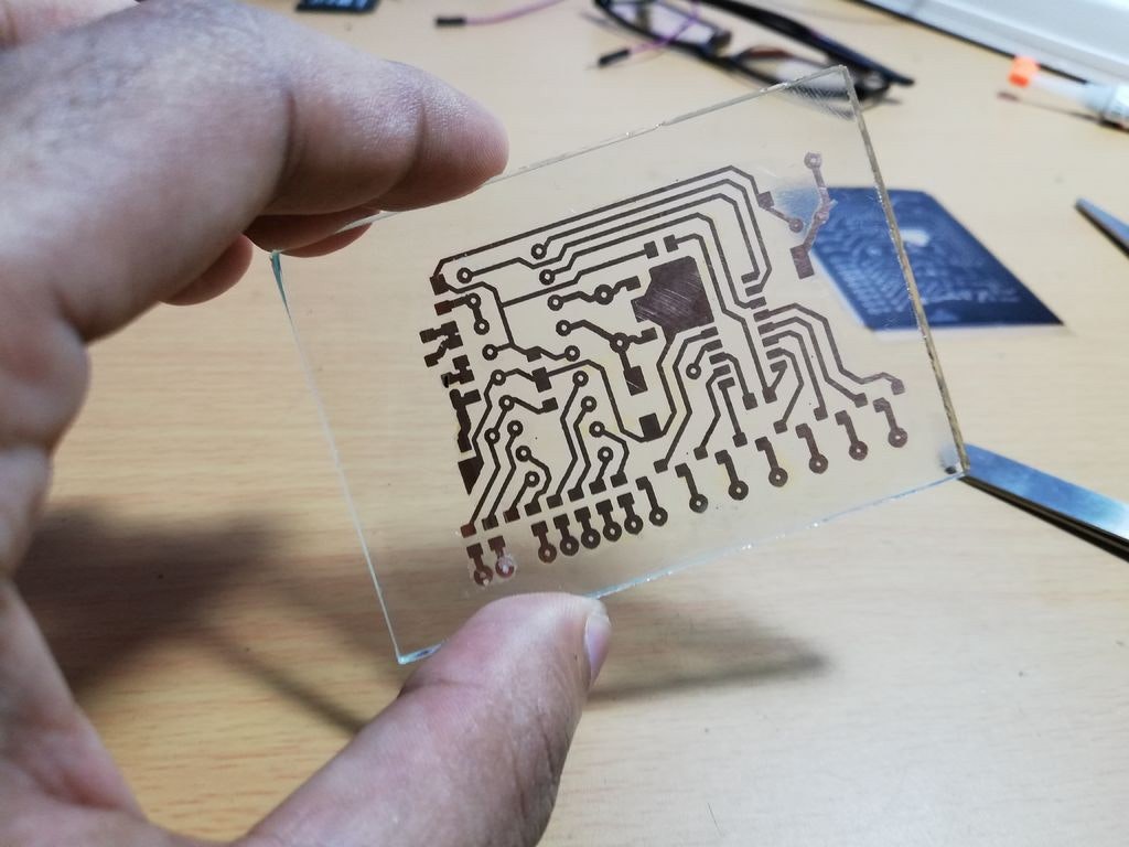
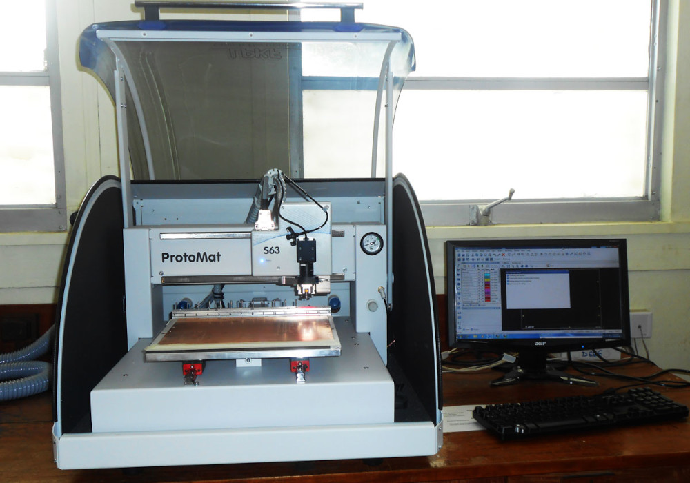
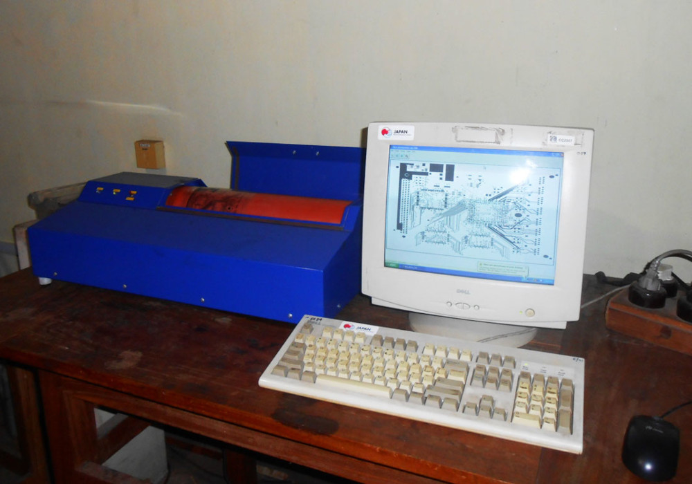
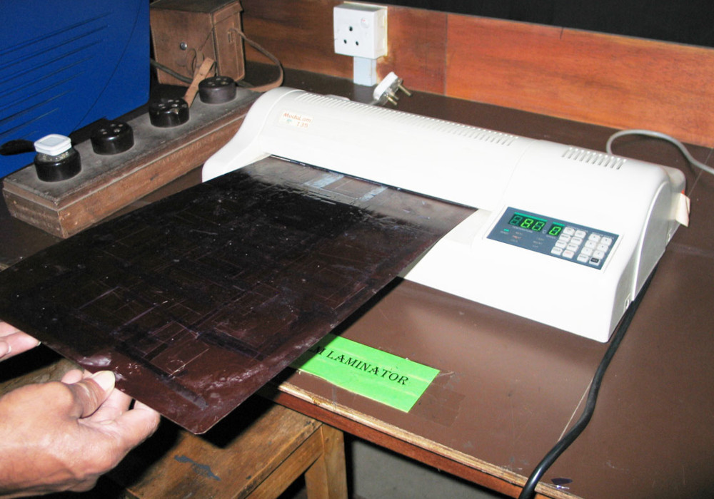
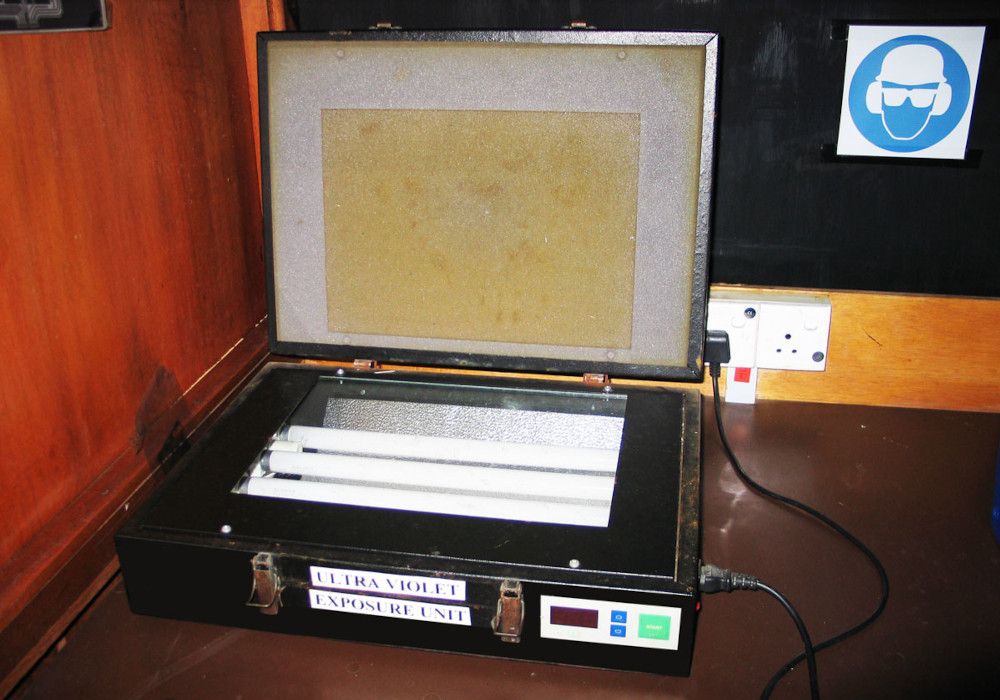
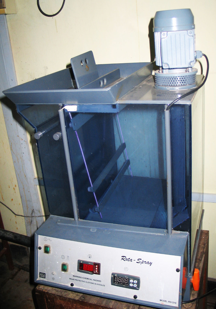
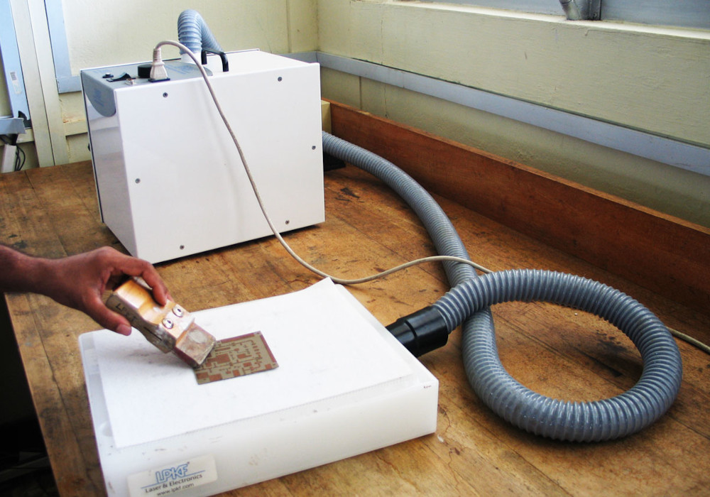
The R&D work of the DEEE is facilitated by a state of the art printed circuit board (PCB) fabrication laboratory. It is a facility dedicated to the design and fabrication of printed circuit boards. It is equipped with a variety of software and hardware resources, including CAD software, 3D printers, and milling machines. The laboratory is used by students and faculty in the electrical and electronic engineering department to design and prototype new electronic devices.
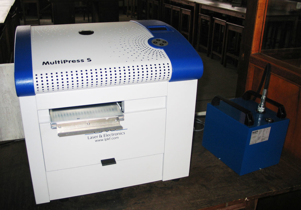
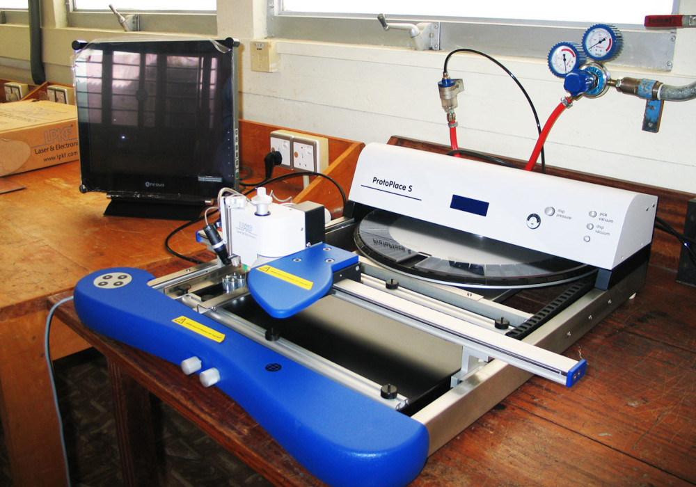
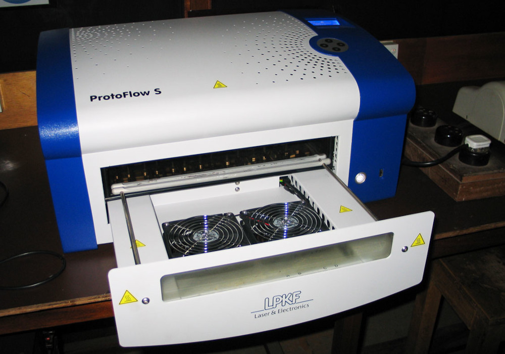
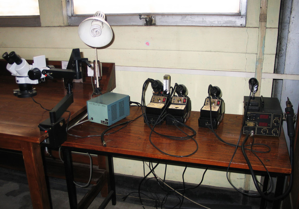
The laboratory is also equipped to handle not only standard FR-4 based PCBs but advance PCBs such as multi-layer boards up to 8 layers, RF and microwave board requiring high precision, and flexible PCBs. The key fabrication techniques used include precision CNC milling and photolithography. The laboratory is also equipped with a pick and place machine, soldering stations for hand soldering, and a re-flow over with programmable temperature profiling.